- 您现在的位置:买卖IC网 > Sheet目录1905 > ATMEGA328P-15AZ (Atmel)MCU AVR 32K FLASH 15MHZ 32-TQFP
2010-2012 Microchip Technology Inc.
DS41413C-page 209
PIC12(L)F1822/PIC16(L)F1823
24.2.5
COMPARE DURING SLEEP
The Compare mode is dependent upon the system
clock (FOSC) for proper operation. Since FOSC is shut
down during Sleep mode, the Compare mode will not
function properly during Sleep.
24.2.6
ALTERNATE PIN LOCATIONS
This module incorporates I/O pins that can be moved to
other locations with the use of the alternate pin function
register, APFCON. To determine which pins can be
moved and what their default locations are upon a
Reset, see Section 12.1 “Alternate Pin Function” for
more information.
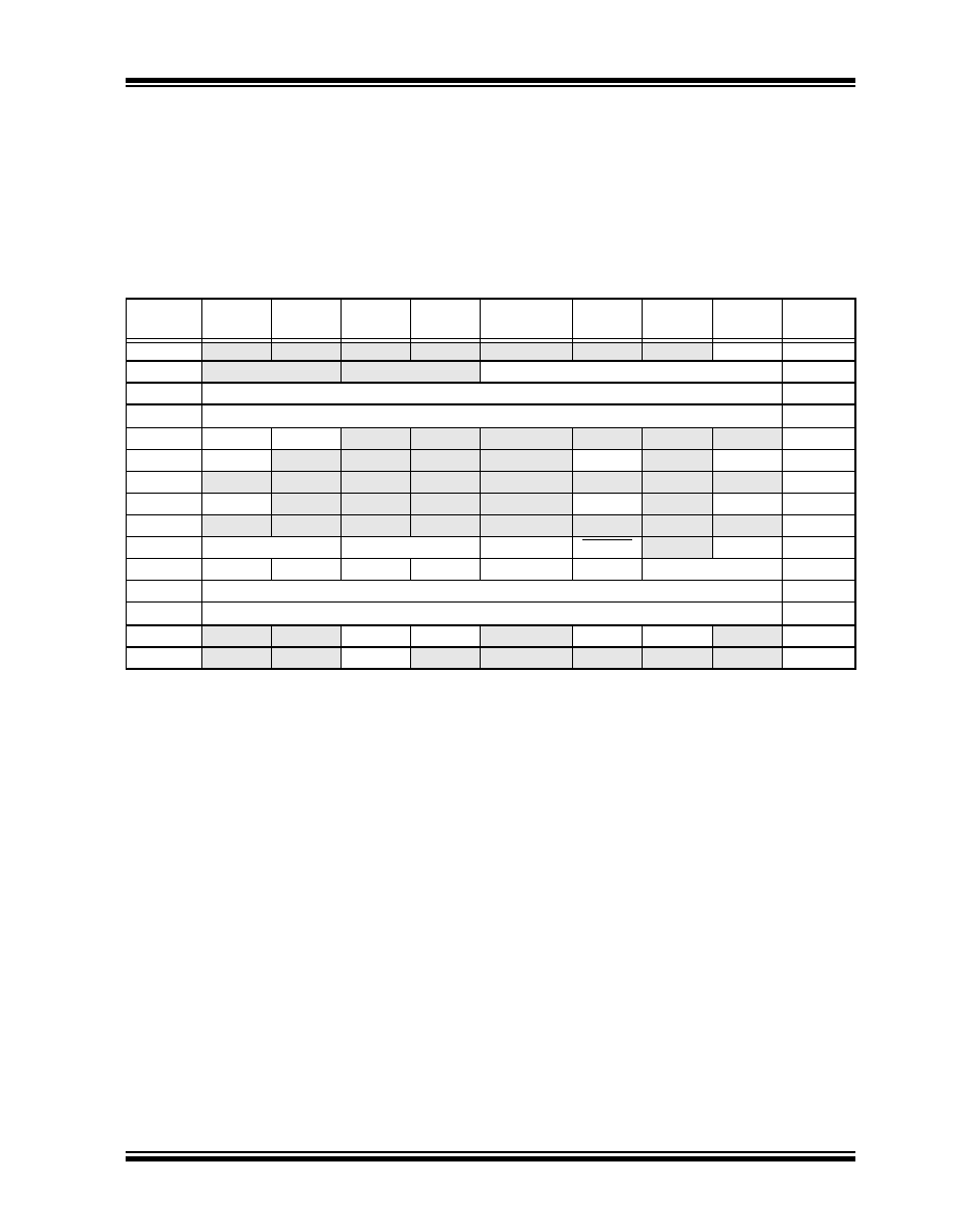
TABLE 24-4:
SUMMARY OF REGISTERS ASSOCIATED WITH COMPARE
Name
Bit 7
Bit 6
Bit 5
Bit 4
Bit 3
Bit 2
Bit 1
Bit 0
Register
on Page
APFCON
RXDTSEL
SDOSEL
SSSEL
—
T1GSEL
TXCKSEL
P1BSEL
CCP1SEL
CCP1CON
P1M<1:0>
DC1B<1:0>
CCP1M<3:0>
CCPR1L
Capture/Compare/PWM Register 1 Low Byte (LSB)
CCPR1H
Capture/Compare/PWM Register 1 High Byte (MSB)
INTCON
GIE
PEIE
TMR0IE
INTE
IOCIE
TMR0IF
INTF
IOCIF
PIE1
TMR1GIE
ADIE
RCIE
TXIE
SSP1IE
CCP1IE
TMR2IE
TMR1IE
PIE2
OSFIE
C2IE(1)
C1IE
EEIE
BCL1IE
—
PIR1
TMR1GIF
ADIF
RCIF
TXIF
SSP1IF
CCP1IF
TMR2IF
TMR1IF
PIR2
OSFIF
C2IF(1)
C1IF
EEIF
BCL1IF
—
T1CON
TMR1CS<1:0>
T1CKPS<1:0>
T1OSCEN
T1SYNC
—TMR1ON
T1GCON
TMR1GE
T1GPOL
T1GTM
T1GSPM
T1GGO/DONE
T1GVAL
T1GSS<1:0>
TMR1H
Holding Register for the Most Significant Byte of the 16-bit TMR1 Register
TMR1L
Holding Register for the Least Significant Byte of the 16-bit TMR1 Register
TRISA
—
TRISA5
TRISA4
TRISA3
TRISA2
TRISA1
TRISA0
TRISC(1)
—
—TRISC5
TRISC4
TRISC3
TRISC2
TRISC1
TRISC0
Legend:
— = Unimplemented location, read as ‘0’. Shaded cells are not used by Compare mode.
Note
1:
PIC16(L)F1823 only.
发布紧急采购,3分钟左右您将得到回复。
相关PDF资料
ATMEGA32L-8PJ
IC MCU AVR 32K 5V 8MHZ 40-DIP
ATMEGA32M1-AUR
IC MPU AVR 32K 20MHZ 32TQFP
ATMEGA48PA-MMNR
MCU AVR 4KB FLASH 20MHZ 28QFN
ATMEGA644P-B15MZ
IC MCU 8BIT 64KB FLASH 32VQFN
ATMEGA644V-10PU
IC AVR MCU FLASH 64K 40DIP
ATMEGA645V-8MI
IC AVR MCU FLASH 64K 1.8V 64QFN
ATMEGA649-16MI
IC AVR MCU FLASH 64K 5V 64QFN
ATMEGA649V-8MI
IC AVR MCU FLASH 64K 1.8V 64QFN
相关代理商/技术参数
ATMEGA328P-15MZ
功能描述:8位微控制器 -MCU 32KB In-system Flash 20MHz 1.8V-5.5V RoHS:否 制造商:Silicon Labs 核心:8051 处理器系列:C8051F39x 数据总线宽度:8 bit 最大时钟频率:50 MHz 程序存储器大小:16 KB 数据 RAM 大小:1 KB 片上 ADC:Yes 工作电源电压:1.8 V to 3.6 V 工作温度范围:- 40 C to + 105 C 封装 / 箱体:QFN-20 安装风格:SMD/SMT
ATMEGA328P-20AU
制造商:Atmel Corporation 功能描述:MCU 8-bit ATmega AVR RISC 32KB Flash 3.3V/5V 32-Pin TQFP
ATMEGA328P20MU
制造商:Atmel Corporation 功能描述:MCU 8-Bit ATmega AVR RISC 32KB Flash 3.3V/5V 32-Pin MLF
ATMEGA328P-AN
功能描述:8位微控制器 -MCU AVR 32K FLSH 2K SRAM 1KB EE-20 MHZ 105C RoHS:否 制造商:Silicon Labs 核心:8051 处理器系列:C8051F39x 数据总线宽度:8 bit 最大时钟频率:50 MHz 程序存储器大小:16 KB 数据 RAM 大小:1 KB 片上 ADC:Yes 工作电源电压:1.8 V to 3.6 V 工作温度范围:- 40 C to + 105 C 封装 / 箱体:QFN-20 安装风格:SMD/SMT
ATMEGA328P-ANR
功能描述:8位微控制器 -MCU AVR 32K FLSH 2K SRAM 1KB EE-20 MHZ 105C
RoHS:否 制造商:Silicon Labs 核心:8051 处理器系列:C8051F39x 数据总线宽度:8 bit 最大时钟频率:50 MHz 程序存储器大小:16 KB 数据 RAM 大小:1 KB 片上 ADC:Yes 工作电源电压:1.8 V to 3.6 V 工作温度范围:- 40 C to + 105 C 封装 / 箱体:QFN-20 安装风格:SMD/SMT
ATMEGA328P-AU
功能描述:8位微控制器 -MCU 32KB In-system Flash 20MHz 1.8V-5.5V
RoHS:否 制造商:Silicon Labs 核心:8051 处理器系列:C8051F39x 数据总线宽度:8 bit 最大时钟频率:50 MHz 程序存储器大小:16 KB 数据 RAM 大小:1 KB 片上 ADC:Yes 工作电源电压:1.8 V to 3.6 V 工作温度范围:- 40 C to + 105 C 封装 / 箱体:QFN-20 安装风格:SMD/SMT
ATMEGA328P-AU SL383
制造商:Atmel Corporation 功能描述:AVR 32K FLASH, 1K EE, 2K SRAM - 20 MHZ, TQFP, IND TEMP GREEN - Tape and Reel
ATMEGA328P-AUR
功能描述:8位微控制器 -MCU AVR 32K FLSH 2K SRAM 1KB EE-20MHz IND
RoHS:否 制造商:Silicon Labs 核心:8051 处理器系列:C8051F39x 数据总线宽度:8 bit 最大时钟频率:50 MHz 程序存储器大小:16 KB 数据 RAM 大小:1 KB 片上 ADC:Yes 工作电源电压:1.8 V to 3.6 V 工作温度范围:- 40 C to + 105 C 封装 / 箱体:QFN-20 安装风格:SMD/SMT